Thursday, December 6, 2018

What is Microcontrollers 8051 Interrupts

Interrupts are the events that temporarily suspend the main program, pass the control to the external sources and execute their task. It then passes the control to the main program where it had left off.
8051 has 5 interrupt signals, i.e. INT0, TFO, INT1, TF1, RI/TI. Each interrupt can be enabled or disabled by setting bits of the IE register and the whole interrupt system can be disabled by clearing the EA bit of the same register.

IE (Interrupt Enable) Register

This register is responsible for enabling and disabling the interrupt. EA register is set to one for enabling interrupts and set to 0 for disabling the interrupts. Its bit sequence and their meanings are shown in the following figure.
IE Register

https://www.tutorialspoint.com/index.htm

What is Microcontrollers 8051 Input Output Ports

8051 microcontrollers have 4 I/O ports each of 8-bit, which can be configured as input or output. Hence, total 32 input/output pins allow the microcontroller to be connected with the peripheral devices.
  • Pin configuration, i.e. the pin can be configured as 1 for input and 0 for output as per the logic state.
    • Input/Output (I/O) pin − All the circuits within the microcontroller must be connected to one of its pins except P0 port because it does not have pull-up resistors built-in.
    • Input pin − Logic 1 is applied to a bit of the P register. The output FE transistor is turned off and the other pin remains connected to the power supply voltage over a pull-up resistor of high resistance.
  • Port 0 − The P0 (zero) port is characterized by two functions −
    • When the external memory is used then the lower address byte (addresses A0A7) is applied on it, else all bits of this port are configured as input/output.
    • When P0 port is configured as an output then other ports consisting of pins with built-in pull-up resistor connected by its end to 5V power supply, the pins of this port have this resistor left out.

Input Configuration

If any pin of this port is configured as an input, then it acts as if it “floats”, i.e. the input has unlimited input resistance and in-determined potential.

Output Configuration

When the pin is configured as an output, then it acts as an “open drain”. By applying logic 0 to a port bit, the appropriate pin will be connected to ground (0V), and applying logic 1, the external output will keep on “floating”.
In order to apply logic 1 (5V) on this output pin, it is necessary to build an external pullup resistor.

Port 1

P1 is a true I/O port as it doesn’t have any alternative functions as in P0, but this port can be configured as general I/O only. It has a built-in pull-up resistor and is completely compatible with TTL circuits.

Port 2

P2 is similar to P0 when the external memory is used. Pins of this port occupy addresses intended for the external memory chip. This port can be used for higher address byte with addresses A8-A15. When no memory is added then this port can be used as a general input/output port similar to Port 1.

Port 3

In this port, functions are similar to other ports except that the logic 1 must be applied to appropriate bit of the P3 register.
https://www.tutorialspoint.com/index.htm

What is Microcontrollers 8051 Pin Description?

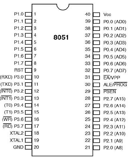
8051 Pin Diagram
  • Pins 1 to 8 − These pins are known as Port 1. This port doesn’t serve any other functions. It is internally pulled up, bi-directional I/O port.
  • Pin 9 − It is a RESET pin, which is used to reset the microcontroller to its initial values.
  • Pins 10 to 17 − These pins are known as Port 3. This port serves some functions like interrupts, timer input, control signals, serial communication signals RxD and TxD, etc.
https://www.tutorialspoint.com/index.htm
What is Microcontrollers 8051 Architecture?

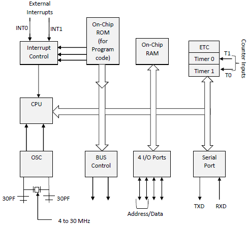
8051 microcontroller is designed by Intel in 1981. It is an 8-bit microcontroller. It is built with 40 pins DIP (dual inline package), 4kb of ROM storage and 128 bytes of RAM storage, 2 16-bit timers. It consists of are four parallel 8-bit ports, which are programmable as well as addressable as per the requirement. An on-chip crystal oscillator is integrated in the microcontroller having crystal frequency of 12 MHz.
In the following diagram, the system bus connects all the support devices to the CPU. The system bus consists of an 8-bit data bus, a 16-bit address bus and bus control signals. All other devices like program memory, ports, data memory, serial interface, interrupt control, timers, and the CPU are all interfaced together through the system bus.
8051 Architecture

https://www.tutorialspoint.com/index.htm
What is Microcontrollers?

microcontroller is a small and low-cost microcomputer, which is designed to perform the specific tasks of embedded systems like displaying microwave’s information, receiving remote signals, etc.
The general microcontroller consists of the processor, the memory (RAM, ROM, EPROM), Serial ports, peripherals (timers, counters), etc.

Difference between Microprocessor and Microcontroller

The following table highlights the differences between a microprocessor and a microcontroller −
MicrocontrollerMicroprocessor
Microcontrollers are used to execute a single task within an application.Microprocessors are used for big applications.
Its designing and hardware cost is low.Its designing and hardware cost is high.
Easy to replace.Not so easy to replace.
It is built with CMOS technology, which requires less power to operate.Its power consumption is high because it has to control the entire system.
It consists of CPU, RAM, ROM, I/O ports.It doesn’t consist of RAM, ROM, I/O ports. It uses its pins to interface to peripheral devices.
https://www.tutorialspoint.com/index.htm

What is Microprocessor - 8257 DMA Controller

DMA stands for Direct Memory Access. It is designed by Intel to transfer data at the fastest rate. It allows the device to transfer the data directly to/from memory without any interference of the CPU.
Using a DMA controller, the device requests the CPU to hold its data, address and control bus, so the device is free to transfer data directly to/from the memory. The DMA data transfer is initiated only after receiving HLDA signal from the CPU.

How DMA Operations are Performed?

Following is the sequence of operations performed by a DMA
  • Initially, when any device has to send data between the device and the memory, the device has to send DMA request (DRQ) to DMA controller.
  • The DMA controller sends Hold request (HRQ) to the CPU and waits for the CPU to assert the HLDA.
  • Then the microprocessor tri-states all the data bus, address bus, and control bus. The CPU leaves the control over bus and acknowledges the HOLD request through HLDA signal.
  • Now the CPU is in HOLD state and the DMA controller has to manage the operations over buses between the CPU, memory, and I/O devices.
https://www.tutorialspoint.com/index.htm

8279 Programmable Keyboard

8279 programmable keyboard/display controller is designed by Intel that interfaces a keyboard with the CPU. The keyboard first scans the keyboard and identifies if any key has been pressed. It then sends their relative response of the pressed key to the CPU and vice-a-versa.

How Many Ways the Keyboard is Interfaced with the CPU?

The Keyboard can be interfaced either in the interrupt or the polled mode. In the Interrupt mode, the processor is requested service only if any key is pressed, otherwise the CPU will continue with its main task.
In the Polled mode, the CPU periodically reads an internal flag of 8279 to check whether any key is pressed or not with key pressure.

How Does 8279 Keyboard Work?

The keyboard consists of maximum 64 keys, which are interfaced with the CPU by using the key-codes. These key-codes are de-bounced and stored in an 8-byte FIFORAM, which can be accessed by the CPU. If more than 8 characters are entered in the FIFO, then it means more than eight keys are pressed at a time. This is when the overrun status is set.
If a FIFO contains a valid key entry, then the CPU is interrupted in an interrupt mode else the CPU checks the status in polling to read the entry. Once the CPU reads a key entry, then FIFO is updated, and the key entry is pushed out of the FIFO to generate space for new entries.
See more info visit : https://www.tutorialspoint.com/index.htm